IMote2 GPIO
Overview
There are two sets of connectors on the iMote2:
- Advanced Connectors made up of a 40pin and a 20pin connector
- Basic Connectors made up of a 31pin and a 21pin connector
The connectors are not symmetric, though some common functions such as deubgging ports, important signals, power, and grounds are shared between the two.
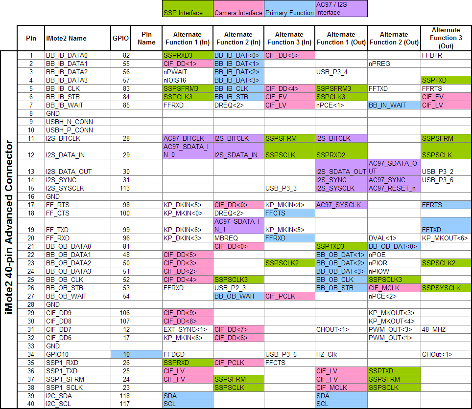
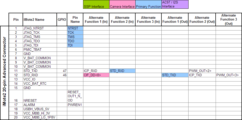
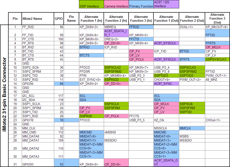
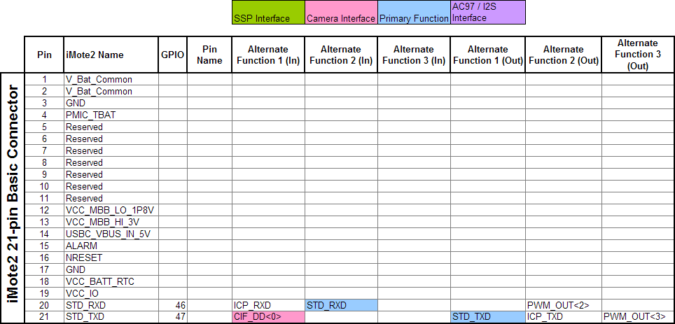
The following charts show the pinouts for each of the connectors along with the corresponding GPIO number and the table of alternate functions.
iMote2 Alternate Functions
Note, although the following are Excel spreadsheets since there's no obviously easy way to get them into Mediawiki they are imported as pictures. Color coding denotes the intended use (according to the pins name on the connectors, in blue) along with some useful secondary functions like SSP, Camera, and AC97/I2S sound interfaces.
Advanced Connector
Basic Connector
Alternate Functions
The XScale processor on the iMote2 is limited by the number of I/O pins that can be practically put on the package. Because the chip is designed to be a general purpose processor some flexibility is added to the system design by making each physical I/O pin capable of performing a number of different operations. I/O pins can be either general purpose input/output pins (GPIO) or special purpose/dedicated bidirectional pins (like serial ports, hi-speed interfaces, etc).
Example GPIO Pin
-
For example, GPIO pin 28 (pin 11/I2S_BITCLK on the 40pin advanced connector) is capable of being:
- A normal GPIO pin (input or output), with programmable interrupts
- Or if needed this pin can be configured as:
- the AC97 Bit Clock
- the I2S Bit Clock
- the Synchronous Serial Port Frame marker output
Register Overview
-
The actual function of the IO pin is set by registers on the chip. On boot, all pins are set as inputs and then can be configured as needed. The registers that control the function of each I/O pins are:
- GPLR Registers - Used to read the state of a GPIO pin
- GPDR Registers - Used to set the direction of a GPIO pin (input or output)
- GPSR Registers - Used to set a output on a GPIO pin (output 1)
- GPCR Registers - Used to clear a output on a GPIO pin (output 0)
- GRER Registers - Used to set an interrupt to detect a rising edge on a GPIO pin
- GEFR Registers - Used to set an interrupt to detect a falling edge on a GPIO pin
- GESR Registers - Used to determine whether an edge detect event has occured on a GPIO pin
- GAFR Registers - Used to set the alternate function of a GPIO pin
Register Details
The following is the documentation provided by the XDB Modify Register tool. For a complete explanation be sure to review the XScale Developer's guide.
The following is a summary only and does not contain all the errata, special conditions, and other considerations a register might have!
GPLR - GPIO Pin-Level Registers
GPIO Pin-Level Registers (GPLR) (0x40E0 0000-08) (0x40E0 0100) (Read Only)

The state of each of the GPIO pins is visible through the GPIO Pin-Level register (GPLR). Each bit
corresponds to the pin number. GPLR0 (31:0) correspond to GPIO[31:0], GPLR1(31:0) correspond to
GPIO[63:32], GPLR2 (31:0) correspond to GPIO[95:64] and GPLR3 (31:0) correspond to GPIO [127:96].
These read-only registers determine the current value of a particular pin (regardless of the
programmed pin direction).

The table below shows the locations of the 32 pin-level bits within the GPLR0. Reads from reserved
 bits (bits 18 through 31 of GPLR3) should be ignored.

Bit n:	Read Only PL{n}
	GPIO pin level n (where n = 0 through 31).
	0 = Pin state is low.
	1 = Pin state is high.
GPDR - GPIO Pin Direction Registers
GPIO Pin Direction Registers (GPDR) (0x40E0 000C-14) (0x40E0 010C)

Users control pin direction by programming the GPIO Pin Direction registers (GPDR0, GPDR1, GPDR2,
GPDR3). The GPDR registers contain one direction control bit for each of the 121 pins. If a
direction bit is programmed to a 1, the port is an output. If it is programmed to a zero, it is
an input.

Note: At reset, all bits in this register are cleared, configuring all GPIO pins as inputs. For
correct operation as an input the RDH bit of the PSSR must be 0 . Reserved bits (bits 18 through
31 of GPDR3), should be written to zeros, and Reads to the reserved bits should be ignored.

The table below shows the location of each pin direction bit in the GPIO Pin Direction register, GPDR0.

Bit n:	PD{n}
	GPIO pin direction n (where n = 0 through 31).
	0 = Pin configured as an input.
	1 = Pin configured as an output.
GPSR - GPIO Pin Output Set Registers
GPIO Pin Output Set Registers (GPSR) (0x40E0 0018-20) (0x40E0 0118) (Write)

When a GPIO is configured as an output, users control the state of the pin by writing to either
the GPIO Pin Output Set registers (GPSR) or the GPIO Pin Output Clear registers (GPCR). An Output
pin is set by writing a 1 to its corresponding bit within the GPSR. To clear an Output pin, a
1 is written to the corresponding bit within the GPCR (write-only registers; Reads return
unpredictable values).

Writing a 0 to any of the GPSR or GPCR bits has no effect on the pin state.

Writing a 1 to a GPSR or GPCR bit corresponding to a pin that is configured as an input will take
effect only after the pin is configured as output. Reserved bits (bits 18 through 31 of GPSR3 and
GPCR3) must be written with 0s; Reads should be ignored. If a 1 is written to both registers at the
same location then the last write takes effect (i.e. an output cannot be both set and cleared at
the same time)

The table below shows the locations of the GPSR0 bits.

Bit n: 	PS{n}
	GPIO output pin set n (where n = 0 through 31).
	0 = Pin level unaffected.
	1 = If pin configured as an output, set pin level high (one)
GPCR - Pin Output Clear Registers
Pin Output Clear Registers (GPCR) (0x40E0 0024-2C) (0x40E0 0124) (Write)

When a GPIO is configured as an output, users control the state of the pin by writing to either the
GPIO Pin Output Set registers (GPSR) or the GPIO Pin Output Clear registers (GPCR). An Output pin
is set by writing a 1 to its corresponding bit within the GPSR. To clear an Output pin, a 1 is
written to the corresponding bit within the GPCR (write-only registers; Reads return unpredictable
values).

Writing a 0 to any of the GPSR or GPCR bits has no effect on the pin state.

Writing a 1 to a GPSR or GPCR bit corresponding to a pin that is configured as an input will take
effect only after the pin is configured as output. Reserved bits (bits 18 through 31 of GPSR3 and
GPCR3) must be written with 0s; Reads should be ignored. If a 1 is written to both registers at
the same location then the last write takes effect (i.e. an output cannot be both set and cleared
at the same time)

The table below shows the locations of the GPCR0 bits.

Bit n:	PC{n}
	GPIO output pin clear n (where n = 0 through 31).
	0 = Pin level unaffected.
	1 = If pin configured as an output, clear pin level low (zero).
GRER - GPIO Rising-Edge Detect-Enable Registers
GPIO Rising-Edge Detect-Enable Registers (GRER) (0x40E0 0030-38) (0x40E0 0130)

GPIO Rising-Edge and Falling-Edge Detect-Enable Registers
Each GPIO can also be programmed to detect a rising-edge, falling-edge, or either transition on a pin.
It is required, however, that the pulse following the edge be AT LEAST 100ns wide to guarantee a
detection. When an edge is detected that matches the type of edge programmed for the pin, a status bit
is set. The Interrupt controller can be programmed to signal an Interrupt to the CPU or wake up the
processor from Sleep mode when any one of these status bits is set. The GPIO Rising-Edge and
Falling-Edge Detect-Enable registers (GRER and GFER, respectively) select the type of transition on a
GPIO pin that causes a bit within the GPIO Edge-Detect Enable Status register (GEDR) to be set. For a
given GPIO pin, its corresponding GRER bit is set to cause a GEDR status bit to be set when the pin
transitions from logic level zero (0) to logic level one (1).
Likewise, GFER is used to set the corresponding GEDR status bit when a transition from logic level one
(1) to logic level zero (0) occurs. When the corresponding bits are set in both registers, either a
falling- or a rising-edge transition causes the corresponding GEDR status bit to be set.

The table below shows both the rising-edge enable bit locations corresponding to all 32 pins of GRER0.
Note: For reserved bits in GRER3 and GFER3, writes should be zeros and Reads must be ignored.

Bit n:	RE{n}
	GPIO pin n rising-edge detect enable (where n = 0 through 31).
	0 = Disable rising-edge detect enable.
	1 = Set corresponding GEDR status bit when a rising edge is detected on
	      the GPIO pin.
GFER - GPIO Falling-Edge Detect-Enable Registers
GPIO Falling-Edge Detect-Enable Registers (GFER) (0x40E0 003C-44) (0x40E0 013C)

GPIO Rising-Edge and Falling-Edge Detect-Enable Registers
Each GPIO can also be programmed to detect a rising-edge, falling-edge, or either transition on a pin.
It is required, however, that the pulse following the edge be AT LEAST 100ns wide to guarantee a
detection. When an edge is detected that matches the type of edge programmed for the pin, a status bit
is set. The Interrupt controller can be programmed to signal an Interrupt to the CPU or wake up the
processor from Sleep mode when any one of these status bits is set.
The GPIO Rising-Edge and Falling-Edge Detect-Enable registers (GRER and GFER, respectively) select the
type of transition on a GPIO pin that causes a bit within the GPIO Edge-Detect Enable Status register
(GEDR) to be set. For a given GPIO pin, its corresponding GRER bit is set to cause a GEDR status bit to
be set when the pin transitions from logic level zero (0) to logic level one (1). Likewise, GFER is used
to set the corresponding GEDR status bit when a transition from logic level one (1) to logic level zero
(0) occurs. When the corresponding bits are set in both registers, either a falling- or a rising-edge
transition causes the corresponding GEDR status bit to be set.

The table below shows the falling-edge enable bit locations corresponding to all 32 pins of GFER0.
Note: For reserved bits in GRER3 and GFER3, writes should be zeros and Reads must be ignored.

Bit n:	FE{n}
	GPIO pin n falling-edge detect enable (where n = 0 through 31).
	0 = Disable falling-edge detect enable.
	1 = Set corresponding GEDR status bit when a falling edge is detected on
	      the GPIO pin.
GEDR - GPIO Edge Detect Status Register
GPIO Edge Detect Status Register (GEDR) (0x40E0 0048-50) (0x40E0 0148)

The GPIO Edge Detect Status Register (GEDR0, GEDR1, GEDR2, GEDR3) contains a total of 121 status bits
that correspond to the 121 GPIO pins. When an edge-detect occurs on a pin that matches the type of
edge programmed in the GRER and/or GFER registers, the corresponding status bit is set in GEDR. Once
a GEDR bit is set, the CPU must clear it. GEDR status bits are cleared by writing a 1 to them.

Writing a 0 has no effect.
Each edge-detect that sets the corresponding GEDR status bit for GPIO pins 0 - 120 can trigger an
Interrupt request. Pins 2- 120 together form a group that can cause one Interrupt request to be
triggered when any one of the GEDR status bits 2- 120 is set. GPIO pins 0 and 1 cause an independent
first-level Interrupt. Refer to Chapter 11, "Interrupt Controller" for a description of the
programming of GPIO Interrupts.

The table below show the GEDR0 bit locations.

Bit n:	Read/Write 1 to clear ED{n}
	GPIO edge detect status n (where n = 0 through 31).
	0 = No edge detect has occurred on pin as specified in GRER and/or GFER.
	1 = Edge detect has occurred on pin as specified in GRER and/or GFER.
GAFR - GPIO Alternate Function Register
GPIO Alternate Function Register (GAFR) (0x40E0 0054-70)

The GPIO Alternate Function registers (GAFR) contain select bits that correspond to the 121 GPIO
pins. Each GPIO can be configured to be either a generic GPIO pin, or for serving up to three
alternate functions as inputs and three alternate functions as outputs. Each GPIO pin has two bits
assigned to it whose values indicate the following:
- 00 indicates normal GPIO function
- 01 indicates alternate function 1
- 10 indicates alternate function 2
- 11 indicates alternate function 3
Note: The power manager can override the alternate function of GPIO[2 - 10] directly.

When the processor sets two bits in the GAFR, the corresponding GPIO pin is switched over to that
pin's alternate function. All GAFR registers are cleared to all zeroes on reset conditions.
GAFR3_U bits 18 to 31 are Reserved.

See the following section for details on alternate functions.
The table below provides bit definitions for the GAFR register.

Bit n:	AF{n}
	GAFR0/1/2/3_L/U bits (where n = 0 through 31).
	A bit-pair in this register indicates that the corresponding GPIO pin is to be
	used for one of the alternate function that is mapped to it or as a generic
	GPIO pin.
	A 00 in this bit-pair indicates that the corresponding GPIO pin is to be used
	       for its normal GPIO function.
	A 01 in this bit-pair indicates that the corresponding GPIO pin is to be used
	       for its alternate function 1.
	A 10 in this bit-pair indicates that the corresponding GPIO pin is to be used
	       for its alternate function 2.
	A 11 in this bit-pair indicates that the corresponding GPIO pin is to be used
	       for its alternate function 3.


